


Design for Testability in Semiconductor Industry

Meta: Present days challenges require modern solutions. DFT solves the probing challenge of dealing with high quantity production without compromising the quality.
Abstract: Design for Testability in Semiconductor Industry provides the much needed breeze to the manufacturers to catch a breath with the increasing demand and pressure for mass production. It helps produce chips with flawless design and impeccable functionality. Here we would get to know a basic overview of what DFT stands for and what is the importance it holds in the semiconductor industry. We would also analyze different testing methods.
With the advancement made in the technology domain, there is a complete paradigm shift in all the sectors. The semiconductor is one of the main catalysts for the technology boom, amongst those. It is poised to grow exponentially with 8.6% CAGR from 2021 to 2028 period with the present market size being USD 425.96 billion. According to research, it has the potential to become worth USD 803.15 billion within 2028.
A semiconductor is the heart of all the advancements made in the electronics industry. With the induction of new technologies such as 14nm or even small nanometer technology, the industry has revolutionized to keep momentum with the demand from the market of enhanced capacity and improved performance. It is projected to fuel further growth momentum of the electronic industry.
What is the buzz about Design for Testability?
Recently, we all have come across DFT or Design for Testability being floated around in the industry as a hot topic. Though it may seem a bit new, it has been there as a prevalent and standard practice to adhere to by the chip manufacturing companies. The introduction of DFT can be seen as more of the aftereffect of time-to-market imperatives. RnD time due to enormous pressure, from the industry demand, often tends to shorten the cycle of the production by letting go of any testing phase which makes a huge issue at a later part when products turn out to be faulty.
Obtaining a prototype to gain a competitive edge becomes so important, that testability requirements do take the backseat. It is also reasoned that once the prototype is done, all the additional features can be added later as per the requirements, but it becomes a pressing bottleneck for the production team when multiple deliveries loom over their heads.
It is indeed a chicken and egg problem for the industry to cater to the fast-paced and exponentially increasing demands from the customers and on the other side, maintaining a strict tab on the production to reduce the number of faulty chips is a herculean task for them. One chip in modern days contains more than 1000 pins. It is like finding a needle in the haystack to find out the faulty pin or part. If quality checks are strictly imposed, then products may never reach the market as promised to render the entire time-to-market useless. That’s where DFT becomes the savior.
DFT takes care of both. In simple terms, Design for Testability or DFT is regarded as a design technique that enables timely chip testing fast enough and cost-effective with the addition of extra circuitry to the chip. Also, the DFT technique improves the controllability and observability of the internal nodes for testing embedded functions. DFT takes 3 parameters as the most important KPIs:
The products need to be tested –
- As fast as possible
- As economical as possible
- As many repeatabilities as possible
It aims to make sure the outcome of the product is fault-free and meeting the requirement of the clients.
Challenges faced by the industry:
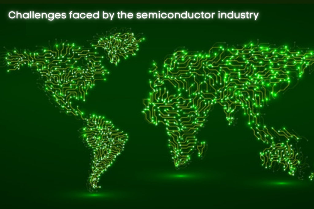
The semiconductor industry is currently going through an overhaul and facing a truckload of challenges to meet the demand from the market without compromising the quality. Few inherent challenges being faced are:
- Application criticality: Few applications are extremely critical and directly related to human lives. Any minor fault can be catastrophic and may end up taking a human life. For instance, any application in the medical field must be perfect, or otherwise, it can prove fatal. Space shuttles that are reliant on cryogenic fuel, need the microcontroller/microprocessor to run on extreme temperature ranges and also to be tested at an extreme level as lives depend on it. These are very application-specific needs and must be dealt with in a certain manner.
- Software problem: Software can become a deterrent too. From fabrication systems to have a bug in the CAD tool, it can affect the chip designing process.
- Density headache: With the deep-submicron design, fabrication has become intensely complex. Chip is becoming thinner and smaller day by day and design elements keep on fighting for tiny little space, resulting in a high chance of collision. In between, two wires touching each other and one getting broken is a very common yet pressing issue. With higher density, the failure probability is also quite high.
Maintenance issue: For maintenance or repair, identifying proper elements and subsequent coordinates of error is a difficult task. Manual testing has lost its sheen as it’s not viable anymore in the case of SCs. So new method of testing is of urgent need.
Challenges faced by the industry:
The semiconductor industry is currently going through an overhaul and facing a truckload of challenges to meet the demand from the market without compromising the quality. Few inherent challenges being faced are:
- Application criticality: Few applications are extremely critical and directly related to human lives. Any minor fault can be catastrophic and may end up taking a human life. For instance, any application in the medical field must be perfect, or otherwise, it can prove fatal. Space shuttles that are reliant on cryogenic fuel, need the microcontroller/microprocessor to run on extreme temperature ranges and also to be tested at an extreme level as lives depend on it. These are very application-specific needs and must be dealt with in a certain manner.
- Software problem: Software can become a deterrent too. From fabrication systems to have a bug in the CAD tool, it can affect the chip designing process.
- Density headache: With the deep-submicron design, fabrication has become intensely complex. Chip is becoming thinner and smaller day by day and design elements keep on fighting for tiny little space, resulting in a high chance of collision. In between, two wires touching each other and one getting broken is a very common yet pressing issue. With higher density, the failure probability is also quite high.
Maintenance issue: For maintenance or repair, identifying proper elements and subsequent coordinates of error is a difficult task. Manual testing has lost its sheen as it’s not viable anymore in the case of SCs. So new method of testing is of urgent need.
Step by Step process of DFT:
DFT test covers the entire 360-degree paradigm of the testing process. From the induction of the testing process to completion, it covers multiple aspects of extensive testing. There are three ways testing is carried out:
- Chip-level: when we manufacture the chips.
- Board-level: When the already manufactured chips get integrated on the board
- System-level: When we assemble all the boards
It is regarded as a rule of thumb that as we move to the next level (Chip -> Board – > System), device testing becomes 10 times more expensive than the previous one as it becomes more difficult at each level to have localization and fault detection.
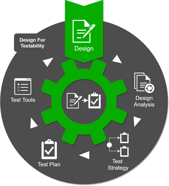
DFT test starts with the design phase and then rigorously goes through 4 steps before it can feedback the required changes in design. It encompasses all the needs for design for testability in VLSI.
Design Analysis:
As the name suggests, in this first step the entire system’s preliminary design is studied – from block diagrams, schematics, to the complete interfaces and how they interact with each other. After this, those findings are traced into a matrix form to document and carry forward to the next steps. It needs to be made sure that schematics have been at the initial level and are open for modification in the later stage.
Test Strategy:
Once the system design has been accounted for, the next viable step is building a test strategy encompassing all the factors, KPIs to define on a high level how the system needs to be tested. The operational test objectives that are crucial to this stage are:
- The entire cost of testing per unit basis
- The complete target volume
- The throughput of target delivery in units (can be of weeks or months)
- The intended extent of the test coverage
Once the objectives are fixed, the decisions need to be made on:
- What would be the level of automated testing?
- Which one would be more suitable to use as preliminary BOM for test – External test equipment or Mechanical text fixture?
- How the production line would be set up?
- What would be the flow of the test in general from initiation to delivery?
The step gives the DFT engineers the confidence that all defined test objectives would be met as per the expectation. From here, multiple strategies can be simultaneously defined and devised to choose the best possible one.
Test Plan:
Once the strategy is selected from the pool of options, it is needed to further elaborate in detail and make it a preliminary test plan. Once the strategy outlines are set, individual subsets are also put in place.
After this, the tools necessary for the testing part need to be listed systematically. These tools can be mechanical, software, or even electronic in nature or in-system / peripheral.
| Test tool type | In-system | Peripheral |
| Electrical | – Probing test points – hardware measures especially for testing such as an ADC – Hardware generating test signals | – Comprising of all needed test equipment (signal generator, multimeter, external controllable sources) |
| Mechanical | – For better test accommodation, the form factor of the electronic card or enclosure modification is needed. | – Mechanical test fixtures |
| Software | – Test functions are merged in API – Test features are merged with operating GUI | – Test software added to the system – Test equipment Automation |
Aggregation of test tools:
A comprehensive test tools list is prepared. It is one of the main crucial steps of DFT and the success or failure of many areas solely depends on it. In this stage, the imperatives of testability are provided back to the system as more of a vicious circle till the desired outcome is generated. R&D plays a huge role here as their advice is most sorted for this matter. Few tools that are added to the list are –
- For the Software stories backlog, in-system software tools need to be incorporated.
- The same goes for hardware for in-system hardware tests. These are verified and validated by the hardware team and then incorporated into the schematics.
- Marketing and design teams jointly evaluate in-system mechanical test tools. Any modification is done in the product form factor, then the drawings would be complete.
Once it is done, the design is then again put to test and iterated through the DFT cycle till every stakeholder conveys their satisfaction.
Is Testability required in FPGA?
A Field-programmable gate array or FPGA in short is defined as a hardware circuit where multiple logical operations can be carried out and these are integrated circuits. With the increasing complexity and issues, the DFT test is a must step for FPGA devices. One of the most crucial issues for FPGA that DFT engineers face is resource and time limitation. Both skilled manpower and computer processors and available memory are hard to get and performing proper testing can be quite difficult.
In a short duration, if the devices need to be tested according to the standards, then DFT is the best viable option for the DFT engineers. With the increased complexity and density, testability in FPGA also needs an overhaul. Different simulation techniques are in place such as Full RTL Simulation, Full-Timing Simulation, Timing simulation of the subsection, Full simulation, timing only on subsection are a few prominent test simulations used for FPGA designs.
What is the simulation in design for testability?
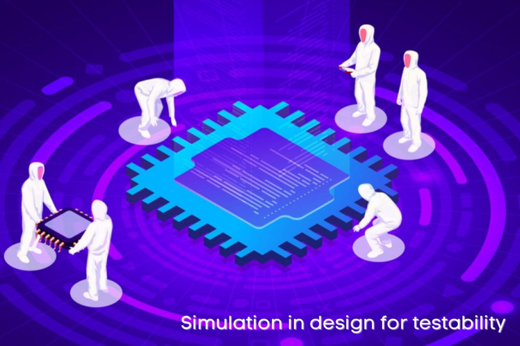
With the modern-day industry demand and the complexities associated with it, DFT engineers are always on the lookout to find out the best possible tests factoring time and operational efficiency. Out of the preferred testing models, timing simulation is the most widely known simulation, but these are also getting limited in performance due to unprecedented complexity.
In present days, both timing and functional simulations are put to test to ensure the quality and design of work. With the pace of new-age and more and more complicated designs are coming up, traditional methodologies of verification are not sufficient anymore. Present days verification processes for testability are:
- Formal Verification or Static Timing Testing:
For verification of expected timing vs desired design, this analysis is used by the engineers. It gives an overall picture of whether the setup can meet the design criteria while keeping other factors static. But it comes with certain limitations such as dynamic factors are not considered here. In real-time situations, there can be multiple time violations due to dynamic factors. Then the simulation technique falls short. For instance, Block Ram collisions with dual-port block Rams, read and write operation can’t be done simultaneously as it will outcome in incorrect data set. Static timing simulations can’t detect it.
- Functional Simulation:
Functional simulation is widely accepted among engineers across the globe. It tests in detail each functionality in RTL design, but it only tests the functional capabilities without counting the timing factor or any changes that have taken place due to optimization and implementation to the original design.
- In-System Testing:
In-System testing is known as the ultimate test that the devices need to go through. This test takes care of the corner-care or hidden issues and once this test is passed, then it is ready for the final release. Though it is widely regarded and renowned in the industry for its finesse, it still holds a bit of drawback. If proper time is not provided to measure each parameter, then the test result might be incomplete and deceptive. All the hardware-related issues need to be fixed before in-system testing begins.
- The hierarchical approach to time simulation:
Keeping a hierarchical approach is the best problem solver the industry can have with modern issues. With the initiation of Verilog and VHDL where HDL is regarded as a coding language, testing has become extremely compact and suitable for modern needs. Choosing a proper hierarchy for testing can change the ball game for testing altogether.