


Distinct Chip level Testing in VLSI
Chip level testing in VLSI: With countless usage of VLSI chips, it is imperative that the chips are completely free of any defect. As the demand has grown exponentially, so is the complexity of new-age chips. Manufacturers are coming up with new testing methods to identify the defect at each stage to provide the best product in the market. Here we will get to know a few prominent Chip level testing in VLSI.
With the revolution of Industry 4.0 and the wide adoption of technology, it has become extremely crucial to launch products with new-age technology prowess and fast go-to-market capabilities. With the rapid and fiercely competitive nature of the market, companies are being mercilessly scrutinized based on their product qualities. Testing has become their best weapon for defense against the threats of faults and errors hidden underneath the perfectly looking products.
Chip level test techniques in VLSI, have been the hot topic in the industry and over the years, it has been gaining traction exponentially. With millions of products being launched every year, testing each product is not a trivial matter, rather a game-changing one. Multiple techniques corresponding to different scenarios and use cases have been introduced. With the shrinking size of the chip or die and the growing complexities, testing needs to cope with the rising challenges.
What is Chip level testing in VLSI trending?
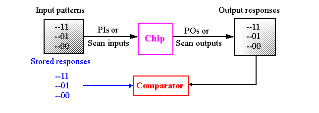
Once the chips are fabricated in VLSI, it is imperative to check their efficacy against the required level of timing and functional specifications. Chip level testing in VLSI in simple terms is providing a predefined set of inputs and matching the outputs against the desired outputs. If the outputs are as per the level of expectation, only then the testing is successful. Testing is not a new concept, since the initiation of VLSI chips, testing has been going on concurrently.
The reason it has been trending across the globe is the business value addition and implication of fast, timely, and accurate testing. The semiconductor industry is being boosted by governments with multiple schemes and as a result, the barrier to entry is coming down drastically. As many startups and companies are coming up in this field, identifying a flaw in the early stage can make or break the game for an organization. Dating back to 1965, Cofounder of Intel, Gordon Moore made a revolutionary prediction about the quantity explosion of transistor numbers. He mentioned that the entire number of transistors incorporated on a die per square inch would grow twice each year.
In the past two decades, every 18 months has become the standard timeline for transistors being doubled. Industry experts do firmly believe that Moore’s law will be relevant at least for another two decades were as predicted, the quantity will grow exponentially but the minimal feature size will decrease and continue to do so. As the transistor size will reduce day by day, the complexity of building such a chip will inherently increase. In addition to that, due to the smaller size, identifying the signal propagation delay would also be difficult which is the main factor for circuit delay determination.
Multiple such probing problems and challenges will come up with the growing number and complexity of the chips and we need to be ready to face such grappling issues. With the advancement in technology and our continuous move towards better and smaller chip designing, multiple new testing use cases will evolve. This will gradually become the emerging factor for chip-building organizations to sustain and thrive.
What is the necessity of timely testing?
As the SoCs are extremely complex in the modern environment, it is important to know the levels of testing and when it should be done along with the business implications. As per the researchers, the questions that need to be asked before testing are:
- What are the functionalities of test chips in designing SoC?
- Is rigorous testing going to be a barrier to time to market?
- Why validation of testing chips is so important relative to the type of IP protocols?
- What are the risks if chips are not properly tested?
There is a simple formula for testing that is followed in the industry:
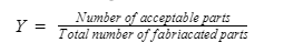
Y is known as the yield or the ratio of acceptance of the parts. Once the technology is new and everything is at a nascent stage, then the yield is as low as 10% but when the technology attains a certain level of maturity, it grows up to a staggering 95%.

As soon as the defect gets detected, it would incur less cost of testing for the final product for the company. The “Rule of Ten” is widely popular in the testing industry about VLSI. It says the testing cost of identifying a defect increases in a magnitude of 10 as the testing phase advances from one stage to another (Chip level – > Board level -> System-level -> System-level at the field). Timely detection can save thousands of dollars for the companies and can save them from missing deadlines.
What are the different types of Chip level testing in VLSI?
As technology has progressed, so has the testing style of chip designing. Complexity has grown immensely, so the test techniques must become unique to meet the challenges of modern days. There are two ways methodically we can segregate the testing process:
Off-chip testing: For this part of testing, external equipment or toolkit is provided to the chip test equipment. One such piece of equipment would be ATE or Automated Test Equipment.
On-chip testing: For this procedure, on the chip or embedded resources are put together to detect any flaw or defect in the circuit.
As per testing circuits, it can be divided into two categories furthermore:
- Combinational Circuit Testing
- Fault Model
- Path Sensitizing
- Sequential Circuit Testing
- Scan Path Test
- Built-In-Self Test (BIST)
- Boundary Scan Test (BST)
Fault Model:
It is noted as the circuit is going to be functionally faulty and incorrect if there is any element wrong in the circuit. There can be multiple categorizations of the fault model:
- Struck at Faults: In case the circuit node gets the logic value fixed permanently, then it can be considered as Struck as Faults.
- Transistor Struck-open faults: In case the transistors are always at the non-conducting level and it seems to be stuck there, it is known as Transistor Struck-open faults.
- Transistor Struck-on faults: This kind of fault is regarded when transistors are always in the conducting stage and thus producing incorrect outputs.
- Delay Faults: Propagation delay is one of the common factors for faulty models. Single propagation delay can cause serious deviation from the desired output (from the specifications of the circuit)
- Bridging Faults: In the case of adjacent nodes, more than often there can be an accidental glitch and as a result, it might produce short-circuit which is known as Bridging faults.
There can be numerous faults, due to complexity and human error. From a mere wire cut to incorrectly connected, transistor switch break and even unwanted connections anything can happen while designing the circuit. Considering multiple factors while testing it can be difficult to perform the test, so for the efficacy, the testing process is restricted to generate the satisfactory result and detect the flaws in the circuitry.
In the case of Struck at models testing, all faults are by default considered as the wire-level and the fault resides at the logic level. For instance, we can consider a wire x. In case, the output is constantly struck at the logic value 0, then we call it struck-at 0, or in the case of logic value 1, we call it struck-at 1.
Path Sensitizing:
It is known as the advanced level of testing compared to the fault model. In a fault model, simple faults are considered, or the efficiency of testing and multiple faults can’t be considered which limits the testing capabilities. In the real world, the chances are, more than often multiple faults will take place concurrently and it needs to be dealt with.
Path Sensitizing does exactly that. It considers multiple faults in use cases and along the path, the signal changes it propagates paves the way for the output. Any deviation is noted and at last with the level of deviation, we can measure what are the faults underlying the circuit design.
Scan Path Testing:
Scan path testing is a part of the sequential testing process where seamless testing of chips is done with flip-flop configuration for serial shift mode. The desired value is gradually shifted by loading the logic values. It is accurately tested by inducing a shift in a special pattern in the scan path even before starting fault method testing.

When test patterns are generated, only flip-flops and I/O pins are considered. When the device is set at the normal mode, then the parallel load is set for mode control but when testing is done, then mode control does frequent alteration between serial shift and parallel load. At the time of operation, normal data is considered with the expected data set to determine the circuit level faults. Few pointers of Scan path testing:
- With automatic test pattern generation, test vectors can also be generated.
- Testers are free of worry about complex test vector generation capabilities regarding the pins of the tested chip.
- Due to the complex testing process, multiplexers need to be added.
Built-in Self-Testing:
As the name suggests, it is designed to be self-sufficient without any human reliance for testing purposes. The test vector generates multiple vectors to be tested for the Circuit In Test. As the intricacies have grown subsequently, testing in simple manners might not be feasible as well as affordable in a fast-paced world. Built-in Self-testing is the answer to the pressing question. Test Generator feeds the input to the Circuit Under Testing and it is constantly monitored by Response Monitor for any error or fault.

Few advantages of BIST are:
- Drastic cost reduction as manual tester involvement is not required.
- High-quality testing whenever required whether it is In-System or At-System.
- In time-sensitive scenarios, it can detect faults faster with ease of diagnosis
- There are no pin or interfacing issues to be bothered about.
- System-level repairing, and maintenance costs are cut down.
Boundary Scan Test:
Though multiple techniques have already been discussed, all of them are applicable for single chips. When it comes to board-level testing or when chips are imprinted on the circuit board, then testing is tremendously complex. To address this issue, the scan-path concept is expanded to the board level to make sure the complexity of VLSI is addressed while testing becomes affordable and more effective.
It is a test technique that extensively uses scan methodology, along with digital devices and services. Scan flip flops are put between internal logic and each device pin. The registers observe and control the signal values present at every input-output level and together they form a register chain. It is known as the boundary scan shift register.
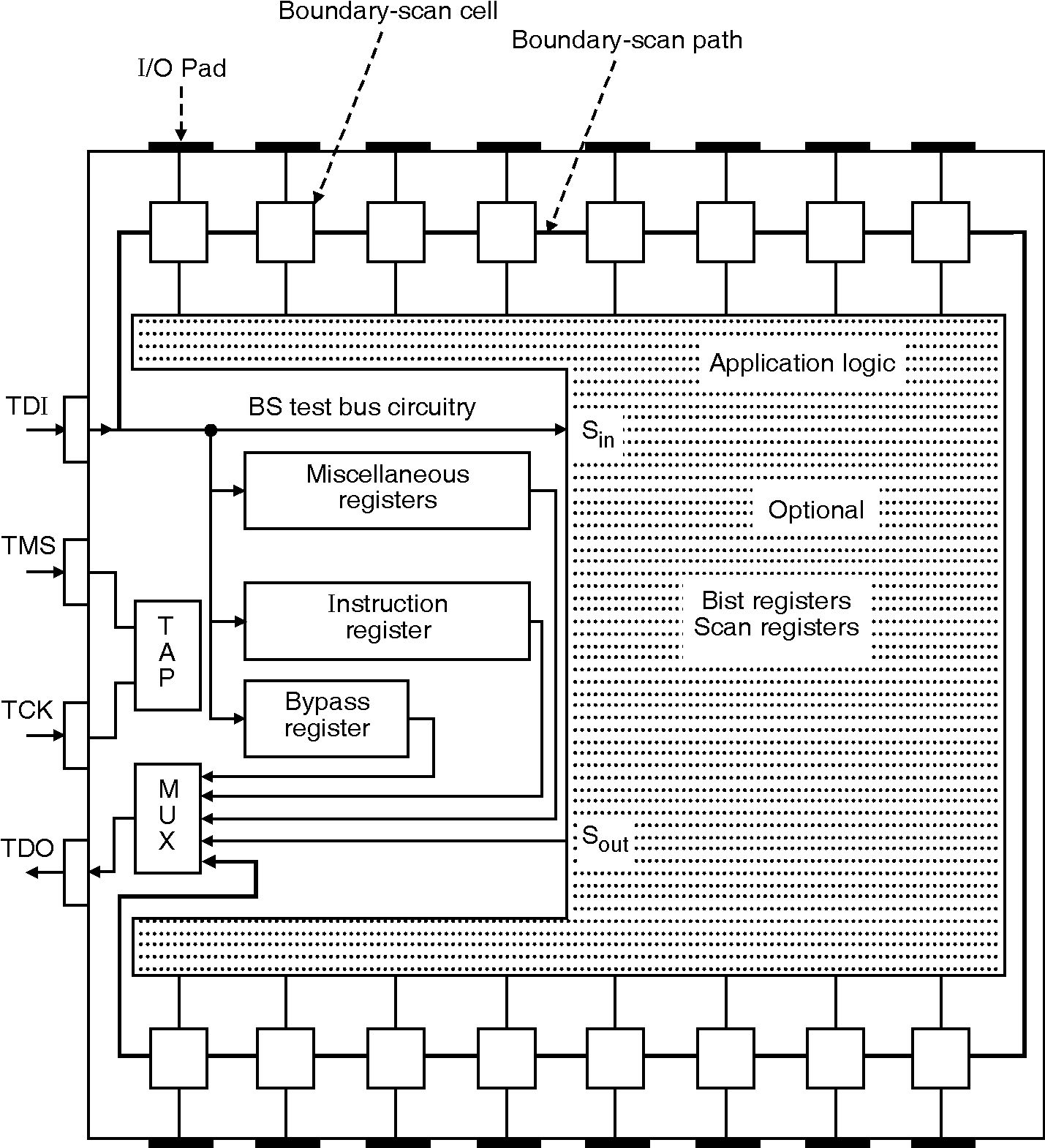
In the register, there are many shift and update stages involved. The update stage with latch specifically stops any output from rippling due to data shifting constantly by the shift register at the time of scan operation. The test stimuli which are put to test in parallel and circuit response can be captured in parallel by boundary scan registers and thoroughly scanned through the scan out port.
The advantages are:
- For PCB testing, the complex testing process can be eliminated and so the need for human intervention can be minimized.
- It eases the job of the test engineer and increases the efficiency multifold.
- Drastically reduces the time spent for complex testing.
- The coverage for all types of faults is expanded heavily.