


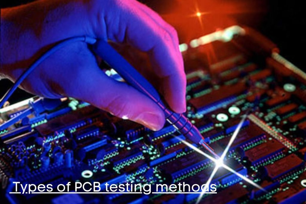
Distinct PCB Testing Methods of Present Days
PCB testing is extremely crucial for having a rapid-scale production of flawless chips. But it is not as simple as it looks. There are multiple use cases and corresponding to that, there are multiple testing methods that check for granular level detailing and analyzes and identifies the flaws if any. In this article, we have compiled a list such 7 testing methods which are popularly used in the industry.
Printed Circuit Boards or popularly known as PCBs are the backbone of the modern-day technology revolution. All the industries are aiming high for the digital revolution and are on their toes to rip every benefit out of it. As the manufacturers are trying their level best to cope with the rapidly increasing demand and the last thing on earth, they want is any failure of their chips. In this highly competitive market, one mistake might completely upend the market share and reputation of the manufacturers.
Keeping up with present-day’s requirements, with numerous components and hundreds of solder connections – rigorous testing has become crucial for the acceptance and success of PCBs. Manufacturers are toiling hard and coming up with new varieties of testing procedures and minute inspection techniques to ensure that PCBs are met with the yardstick of quality parameters and checks. To increase the efficacy and device reliability, every PCB needs to go through a rigorous inspection and testing process based on its specific performance and design standards.
What are PCB inspections and testing?
PCB inspection and testing is a plethora of checks and detailed inspections done to ensure that everything stays as per the plan and there is no room for any flaws or mistakes. To make it work, a yardstick of quality parameters based on functionality and design is set, and PCB standards revolve around those measures. Electric board testing and multiple other testing methods are put to use to perform these testing parts. As it evaluates several main components of PCBs, it ensures that every component is in detail analyzed and tested against the standards. The components that are tested:
- Copper Plating: The copper foil provides the necessary conductivity and is laminated for use. For the PCB to work, the elongation and tensile strength are analyzed rigorously.
- Lamination: Lamination is one of the most integral parts for checking the lifespan of PCBs – if it is not done properly, it can cause serious distress in the overall board functionality. Its resistance to force and heat are checked thoroughly.
- Hole wall quality: While in the field, hole walls should get cracked as the sustainability and durability of PCB depend on it. It is normally analyzed in detail with frequently changing environments to ensure that it doesn’t give up on thermal stress.
- Solderability: Solderability checks whether the components can be incorporated firmly into the PCB. Along with the soldering defects identification, the wetting test is also done which checks for the acceptance of the liquid solder on the surface.
- Electrical Conductivity: One of the most crucial yet undermined areas for PCB. How the electric current passes through CB without causing havoc, is the main subject for this conductivity test.
- Environment: PCBs work in different climates and rough terrain. How tough and durable it is to function under extreme weather conditions is checked here. For this, the PCB is weighed in before and after the test in a humid environment and any minute weight change is also observed and taken into consideration.
Benefits of PCB Testing:
PCB testing is a must for all the manufacturing companies for all the benefits and advantages it provides them. From both technical and business aspects, it has certain tricks under its’ sleeve:
- Identification of bugs is the main reason for PCB testing. Identifying where the bug lies in the half job done. Whether it is manufacturing, designing, or functionality -understanding the nature of it helps to rectify the mistakes.
- As early as the bug gets detected, the precious time gets saved. If the detection is early, it is easy to correct the mistake and fix the issue, however, in case it gets detected at a later stage, then adjusting would be difficult.
- The last thing manufacturer or designer wants is a faulty product in production. PCB testing does the much-needed job of preventing any wasteful production of faulty products. Having the tests done at an early stage, designers and manufacturers can ensure the quality is flawless before it goes for full-scale rapid production mode.
- In case of defective devices, the companies have no other option than to recall the products. It makes a devastating impact on the trust factor and the brand image of the organization. As few goods would be returned, it would be better for from the business perspective.
- With electronic technology, there is always a chance of hidden and underlying danger. These boards are highly inflammable and can wreak havoc damages both on the plant and the workers. Having rigorous testing in place minimizes the chances of any such damage whatsoever.
What are the different types of PCB testing methods?
There are multiple methods in place to check the structure and durability and detect any flaws, if any however, there are few most prominent and popular methods that stand out in the industry level applications:
Visual Inspection:
Visual inspection is the most basic and simplest form of PCBA inspection. With the help of a magnifier, the technician relies solely on his skillset and tries to identify any defect in the solder or components’ misplaced orientation, missing parts, or even board stains.
Advantages:
- If the technician is skilled, many defects can be identified at a very early stage.
- Very easy to set up and scale as the cost is very low compared to other methods.
Disadvantages:
- Extremely labor’s skill-intensive and time-consuming
- It is not free from the possibility of human error
- Only visible flaws can be identified – in case of hidden and underside solder joints can’t be detected with this method.
Use cases:
- Large components with simple designs would be ideal for this testing. Also, in case if it is done in limited quantities, the efficacy increases significantly.
In-Circuit Testing (ICT):
In-circuit testing is a form of automated testing and is extremely popular in the industry due to its high efficiency and coverage for mature products and large batches. With a staggering rate of 90% fault coverage, it can get into the intricacies of PCBA testing which are invisible to the naked eye and identify the hidden flaws instantly. During this test, electrical probes check the specific test points by sending currents in a very systematic manner on the board. It can identify flaws like short circuits, open circuits, misplaced orientation of crucial components like diode or transistors, solder defects.
In case of larger quantities or repetitive batches, customized jigs can do the testing in a faster manner than the normal way.
Advantages:
- Extremely high and accurate fault coverage. (>90%)
- Quick and efficient in testing in large quantities
Disadvantages:
- Test jigs are quite expensive.
- It is not suitable for small quantities or prototype testing.
- Only designated test points can be accessed.
- Certain nature flaws can’t be identified such as voids or insufficient solders.
Use cases:
- Mature products and large volumes would be the ideal use case for this testing methodology.
Flying Probe Testing:
FPT is considered the advanced version of ICT testing. Apart from designated test points, it can use vias and component pads as test points and is extremely cheap to use as there is no need for any customized fixture. The only change from time to time for different types of testing is the upgrade of software and that’s all.
It is extremely useful for finding the orientation of diode or transistor, voltage measurements, and passive parts.
Advantages:
- Extremely fast in implementation. No customized fixture is required.
- Test coverage is comparatively higher than ICT.
Disadvantages:
- Mast testing slows down its speed drastically.
- Certain defects can’t be identified.
Use cases:
- Small and medium levels of production or prototypes with a high level of component density would be ideal for FPT.
Automated Optical Inspection:
AOI is completely next level when it comes to PCB testing. It takes high-resolution pictures with 2D or 3D cameras and then compares and contrasts with the design template board images or with an extensive database of images. It is often known as the first line of quality checks as it gets directly added to the production line. It analyzes and suggests certain changes in the production process.
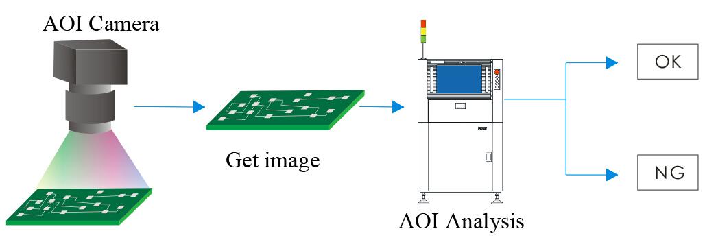
It covers the entire 360-degree aspects of the testing cycle. It can identify most of the visibly indifferentiable components with high efficacy and accuracy.
Advantages:
- Solder defects can easily be detected and better than previous versions of testing.
- Direct addition to production line results in early detection of flaws.
Disadvantages:
- It’s a passive testing methodology. Normally useful only for surface defects.
- The template matching process is time-taking and laborious.
- High dependency on a database might reduce its accuracy due to faulty or low-quality databases.
Use cases:
- Mature products at the production line in high quantity are the ideal use case for this.
Automated X-Ray Inspection:
As the name suggests, the usage of X-Ray makes it unique amongst other testing processes. It can directly create 2D or 3D images of solder joints. In case any joint is hidden from other testing and underlying in Ball Grey Arrays, it can easily identify those along with solder voids.
Due to its high efficacy and unique prowess of finding out hidden defects, added to the production line gives manufacturers the leverage of early detection. Once detected, the engineers can adjust the process accordingly and fix the issues. It greatly reduces pricey repairs. It is also useful in the case of prototypes or small batches.
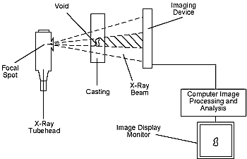
Advantages:
- Among all the other tests, it has the highest detection rate.
- Not only the connection part but long-time solder joints are also taken into consideration for this testing.
Disadvantages:
- Only skilled operators can perform this test properly.
- Quite expensive and time-taking methodology.
Use cases:
- Complex PCB designs and high production volume.
Burn-In Testing:
This testing is like military testing among all. It subjects the PCB boards to extreme weather conditions to find out any hidden flaws or performance issues before tested PCBs go out on the field for their respective use. Its’ core area of strength lies in detecting the early stages of possible failures, load capacity of testing to remove any premature cases of failure in the field. Where other testing methods go for indicators of might-be failures, it simulates the extremely rough conditions like sudden temperature rising, voltage frequency, or design-related conditions.
It collects precise data about the tenacity and rigor of the tested PCBs and with the help of this data, engineers can optimize the designing part.
Advantages:
- It checks the PCBs in rough and realistic conditions, where other testing methods fall short.
- Product reliability is much higher than any other testing method.
Disadvantages:
- Extremely rough testing can do more damage than good to products – like overall yield reduction or lifespan of the product.
- Much expensive and time-consuming testing process.
Use cases:
- Specific use cases where failure can’t be tolerated such as in a military or medical field. This testing becomes extremely relevant in that cases.
Functional Testing:
It is the last stage of production cycle testing. Its job is to ensure that the device put under test can perform as it is intended to be. It is quite flexible. Based on the design complexity or varied testing needs, it can either be extremely simple such as an on-off power test or a complete elongated version of testing with all the necessary protocols and testing software.
It can also be considered as an alternative version of testing for costly testing methods. It can simulate the realistic operating environment for testing and can be more direct than other testing processes. Though finding the early-stage flaws and performing the root cause analysis is not its’ strong suit. It makes sure that each board out of the production cycle is in the ideal operational form.
Advantages:
- Extremely flexible and can be completely tailor-suited for different testing conditions.
- Cost-effective and accurate technique compared to the many other versions.
Disadvantages:
- It’s a skilled man’s job. A high level of training is required to perform this.
- Under stress testing, it can still fall short of identifying certain flaws.
Use cases:
Ideal for low quantities of manufacturing or add-on with other testing methods.